Memory Stage
LSU (Load Store Unit)
In RISC-V core, the Load Store Unit (LSU) is a critical pipeline component responsible for controlling load and store instructions and handling various error conditions, particularly address misalignment. The LSU acts as an interface between the processor’s execution stage and the Memory Management Unit (MMU), ensuring proper data transfer, address calculation, and exception handling.
LSU Queue: The
LSUimplement internal queue to store all necessary dtat for memory operactions.Address Misaligned: In this part, we want LSU detect misaligned error and solve it. Therefore, we need to record every condition, including memory addresses, data values, instruction types, and control signals.
Writeback Data Calculation: This part is for load instruction. In our design, lsu will sent read word signal to mmu even if instruction is
WBorWH. Therefore, it needs caculate word data after lsu get terget data.
Implement Detail
Parameter
Parameter |
Description |
|---|---|
LENGTH |
Queue length parameter |
DEPTH |
Queue depth parameter |
DATASIZE |
Internal data size for queue operations |
Address and Data Procressing
Address: LSU will control address which will be sent into MMU be mutiple of 4.
Data: LSU use mask to control which byte of write data are needed to be writen into memory.
LSU Queue
Queue store data which generate according to input opcode and singal.
Push: input instruction is valid, and misaligned condition.
Pop: when memory return finished signal.
Store Data:
Signal |
Width |
Description |
|---|---|---|
mem_addr |
32 |
Target memory address |
mem_data |
32 |
value of write data |
lb_inst, lh_inst, lw_inst |
1 |
Load instruction type |
signed_inst |
1 |
load instruction is signed |
mem_rd, mem_wr |
1 |
memory read and write signal |
mem_mask |
4 |
store or load mask |
u_type |
1 |
additional instruction for misaligned problem |
Address Misaligned
The LSU includes sophisticated misalignment detection and correction logic. When misaligned memory accesses are detected, the LSU automatically:
Splits the misaligned access into multiple aligned memory transactions
Maintains state information across multiple memory cycles
Reconstructs the final result from partial memory responses
Ensures atomicity of the original memory operation from an architectural perspective
The LSU handles unaligned memory accesses by splitting them into multiple aligned accesses:
Unaligned Detection
Half-word unaligned: Address bits [1:0] = 2’b11
Word unaligned: Address bits [1:0] ≠ 2’b00
Unaligned Access Handling: Maintains state machine (u_state) for multi-cycle unaligned operations. Then, automatically generates second memory access for unaligned transfers.Finally, reconstructs data from multiple memory responses in writeback calculation.
Writeback Value Calculation
For load instructions, the LSU performs intelligent data processing since it always requests full 32-bit words from the MMU regardless of the actual load instruction type (LB, LH, LW). The writeback calculation unit:
Extracts the relevant bytes from the loaded word based on address and instruction type Performs sign extension or zero extension as required Handles data reconstruction for misaligned accesses Manages the timing of writeback operations to the register file
Exception Handling
In this part, LSU will receive signal load_fault and store_fault which is sended from MMU. Then, LSU will generate exception signal with current load or store instruction.
MMU (Memory Management Unit)
In RISC-V core architectures, the Memory Management Unit (MMU) serves as a critical component responsible for translating virtual addresses into physical addresses. Beyond basic address translation, the MMU provides essential security and reliability features through comprehensive error detection mechanisms, including address range validation and page accessibility verification. Our MMU design implements a three-tier architecture comprising specialized units that work in concert to deliver efficient virtual memory management:
Architecture
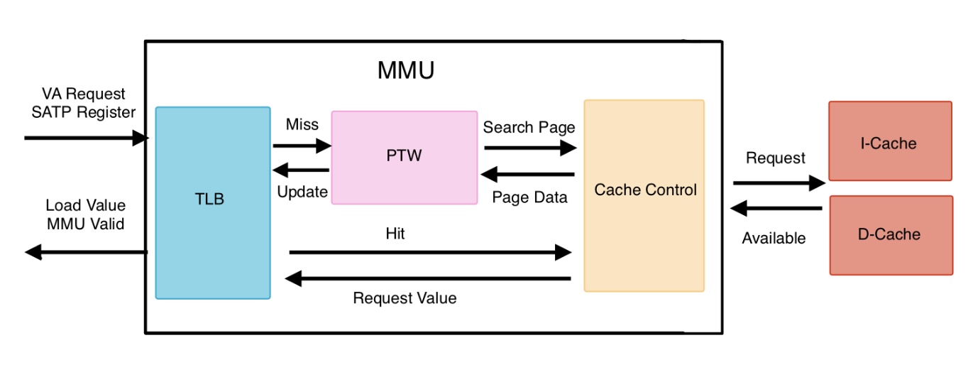
Modules:
mmu_tlb.v: TLB store a history data of pages. It returns value if page was requested, or sent request signal into TLB to find correct page and its data.mmu_ptw.v: PTW can find the correct page with page index of virtual address and calculate physical address by page data. Then, page fault exceptions also are detected in this unit.mmu_cache_control.v: cache control is interface for Dcache and Icache. It receives available signal from cache and sents control signal such as valid signal to control MMU current request is finished.
Implement Detail
TLB
Use two register to store page value, and it compares input virtual page number and vpn_q. If TLB hit, TLB will return page value directly. Otherwise, MMU will start PTW to find target page and update TLB data.
Register |
Width |
Description |
|---|---|---|
vpn_q |
20 |
virtual page number |
entry_q |
32 |
page entry data |
PTW
Page table walker (PTW) can search page table and detect page errror condition. In our virtual address design, we use two level page to translate virtual address into physical address. Therefore, PTW use four state finite state machine to control procession of searching page. Four state include:
State |
Description |
|---|---|
IDLE |
wait MMU start PTW |
FIRST_LEVEL |
search first level page |
SECOND_LEVEL |
search second level page |
UPDATE |
get page data and update TLB |
Virtual Memory (Sv32)
We use Sv32 as our virtual address design. Sv32 use two-level page to translate virtual address into physical address. This is its virtual address structure:
31 - 22 |
21 - 12 |
11 - 0 |
|---|---|---|
First Level Page Index |
Second Level Page Index |
Offset |
Page Table Structure:
Bit Position |
Macro Name |
Description |
|---|---|---|
0 |
PRESENT |
Page is valid in memory |
1 |
READ |
Page has read permission |
2 |
WRITE |
Page has write permission |
3 |
EXEC |
Page has execute permission |
4 |
USER |
Page is accessible in user mode |
5 |
GLOBAL |
Page is global (not flushed on context switch) |
6 |
ACCESSED |
Page has been accessed |
7 |
DIRTY |
Page has been modified |
9:8 |
SOFT |
Software-defined bits (2 bits) |
29:10 |
ENTRY |
Physical page number |
SATP (Supervisor Address Translation and Protection): It is a register to store virtual address information and control page management, and it maintain by CSR. This is Satp structure:
31 |
30 - 22 |
19 - 0 |
|---|---|---|
MODE |
ASID |
PPN |
MODE: virtual address support in current.
ASID: address space identifier to control that address can be used in current process.
PPN: first level physical page number.
Dcache
1. I/O port
System Ports
I/O |
name |
width |
purpose |
|---|---|---|---|
input |
clk |
1 |
Timing |
input |
rst_n |
1 |
Reset dcache at low |
CPU Ports
I/O |
name |
width |
purpose |
|---|---|---|---|
input |
cpu_daddr_i |
32 |
Ports receive a specific address from the CPU |
input |
cpu_data_i |
32 |
Ports receive specific data from the CPU |
input |
mask_i |
4 |
A word is 4 bytes in 32-bit CPU and mask_i is a filter to choose which bytes need to be operated |
input |
cpu_req_wr |
1 |
CPU wants to write data to the cache |
input |
cpu_req_rd |
1 |
CPU wants to read data from the cache |
output |
cpu_data_o |
32 |
Turn specific data back to the CPU |
output |
dcache_rdy_o |
1 |
A handshake telling CPU if this cache is available or not |
output |
dcache_vld_o |
1 |
A handshake telling CPU if this cache completes its work |
output |
d_exception |
2 |
Indicates whether a store or load access fault has occurred |
input |
invalidate_i |
1 |
Invalidate specific cacheline |
input |
flush_i |
1 |
Flush specific cacheline |
input |
writeback_i |
1 |
Write all of the data back to DRAM |
Memory Ports
I/O |
name |
width |
purpose |
|---|---|---|---|
output |
mem_addr |
32 |
Tell DRAM which address cache wants to write or read |
Read
I/O |
name |
width |
purpose |
|---|---|---|---|
input |
rm_rdy |
1 |
A handshake signal to inform the cache if it can send new data to the next stage |
input |
rm_data |
256 |
Data from DRAM |
input |
rm_success |
1 |
Asserted on successful cache read |
input |
rm_complete |
1 |
Asserted when the cache read operation completes. |
output |
rm_vld |
1 |
Notify the bridge to start a read transaction |
Write
I/O |
name |
width |
purpose |
|---|---|---|---|
input |
wm_rdy |
1 |
A handshake signal to inform cache if it can send new data to the next stage |
output |
wm_data |
256 |
Data to DRAM |
input |
wm_success |
1 |
Asserted on successful cache write |
input |
wm_complete |
1 |
Asserted when the cache write operation completes |
output |
wm_vld |
1 |
Notify the bridge to start a write transaction |
2. Description
This is a 32KB 2-way Set-Associative Cache. The storage is implemented using Single-Port BRAM IPs. Each Cache Line size is 256 bits (32 bytes), matching the AXI4 burst width. It employs a Least Recently Used (LRU) replacement policy and a Write-back + Write-allocate strategy to optimize bus bandwidth.
Dcache_axiBus_bridge
1. I/O port
System Ports
I/O |
name |
width |
purpose |
|---|---|---|---|
input |
aclk |
1 |
Timing |
input |
aresetn |
1 |
Reset at low |
Data Cache Ports
I/O |
name |
width |
purpose |
|---|---|---|---|
output |
mem_addr |
32 |
Tell DRAM which address cache wants to write or read |
Read
I/O |
name |
width |
purpose |
|---|---|---|---|
output |
rm_rdy |
1 |
A handshake signal to inform the cache if it can send new instruction to the next stage |
output |
rm_data |
256 |
Data from DRAM |
output |
rm_success |
1 |
Asserted on successful read |
output |
rm_complete |
1 |
Asserted when the read operation completes. |
input |
rm_vld |
1 |
A handshake signal to notify the bridge that a new instruction is available |
Write
I/O |
name |
width |
purpose |
|---|---|---|---|
output |
wm_rdy |
1 |
A handshake signal to inform cache if it can send new instruction to the next stage |
output |
wm_data |
256 |
Data to DRAM |
output |
wm_success |
1 |
Asserted on successful write |
output |
wm_complete |
1 |
Asserted when the write operation completes |
input |
wm_vld |
1 |
A handshake signal to notify the bridge that a new instruction is available |
AXI Ports(Only important ports)
AW Channel
I/O |
name |
width |
purpose |
|---|---|---|---|
output |
M_AXI_AWADDR |
32 |
Tell DRAM which address cache wants to write |
input |
M_AXI_AWREADY |
1 |
Asserted when the write address channel is available |
output |
M_AXI_AWVALID |
1 |
Asserted when the bridge wants to write address to dram |
W Channel
I/O |
name |
width |
purpose |
|---|---|---|---|
input |
M_AXI_WREADY |
1 |
Asserted when the write channel is available |
output |
M_AXI_WDATA |
256 |
Data to DRAM |
output |
M_AXI_WVALID |
1 |
Asserted when the bridge wants to write data to dram |
output |
M_AXI_WLAST |
1 |
Asserted when the data is the last data block of a burst |
B Channel
I/O |
name |
width |
purpose |
|---|---|---|---|
input |
M_AXI_BRESP |
2 |
Indicated whether the write behavior is sucessful |
input |
M_AXI_BVALID |
1 |
Asserted on successful write |
output |
M_AXI_BREADY |
1 |
Asserted when the bridge is available to receive new instruction |
AR Channel
I/O |
name |
width |
purpose |
|---|---|---|---|
output |
M_AXI_ARADDR |
32 |
Tell DRAM which address cache wants to read |
input |
M_AXI_ARREADY |
1 |
Asserted when the read address channel is available |
output |
M_AXI_ARVALID |
1 |
Asserted when the bridge wants to read address from dram |
R Channel
I/O |
name |
width |
purpose |
|---|---|---|---|
input |
M_AXI_RDATA |
256 |
Data from DRAM |
input |
M_AXI_RRESP |
2 |
Indicated whether the read behavior is sucessful |
input |
M_AXI_RLAST |
1 |
Asserted when the data is the last data block of a burst |
input |
M_AXI_RVALID |
1 |
Asserted on successful read |
output |
M_AXI_RREADY |
1 |
Asserted when the bridge is available to receive new instruction |
2. Description
The bridge is responsible for translating the custom D Cache memory interface into the standard AXI4 Full Protocol.
Independent Channel Design: To maximize throughput and exploit AXI parallelism, this bridge implements independent control logic for all five channels (AW, W, B, AR, R). This allows the system to issue new read/write addresses while data transfers are still in progress.
Handshake Protocol: The implementation strictly adheres to the AXI4 handshake rules: VALID signals never wait for READY to be asserted, preventing potential deadlocks in the system.
Design Philosophy: While this design prioritizes performance through independent channels, it serves as an educational reference. For simpler designs or area-constrained environments, AMD/Xilinx also suggests implementing a Single Sequence FSM to handle the channels sequentially, which reduces logic complexity at the cost of concurrency.
I cache
1. I/O ports
System Ports
I/O |
name |
width |
purpose |
|---|---|---|---|
input |
clk |
1 |
Timing |
input |
rst_n |
1 |
Reset icache at low |
CPU Ports
I/O |
name |
width |
purpose |
|---|---|---|---|
input |
pc_i |
32 |
Program counter |
input |
invalidate_i |
1 |
Command to invalidate all cache lines |
output |
icache_rdy_o |
1 |
Indicates if I-cache is ready to accept a new PC |
output |
cpu_inst_o |
32 |
Output particular instruction |
output |
icache_vld_o |
1 |
Indicates the output instruction is valid |
output |
i_exception |
1 |
Indicates a fetch access fault |
Memory Ports
I/O |
name |
width |
purpose |
|---|---|---|---|
output |
mem_addr |
32 |
Tell DRAM which address cache wants to write or read |
Read
I/O |
name |
width |
purpose |
|---|---|---|---|
input |
rm_rdy |
1 |
Indicates the AXI Bridge is ready to process a read request |
Output |
mem_addr |
32 |
Target DRAM address for cache line refill |
input |
rm_success |
1 |
Confirms a successful read transaction from DRAM |
input |
rm_complete |
1 |
Indicates the burst read operation is finished |
input |
rm_data |
256 |
The 256-bit cache line data returned from DRAM. |
output |
req_rm |
1 |
Request signal to read instruction from dram |
2. Description
This is a 16KB 2-way Set-Associative Cache. The storage uses BRAM IPs, with a Cache Line size of 256 bits (32 bytes). It employs a First-In-First-Out (FIFO) replacement policy. To support fast context switching and software reloads, it integrates a DFF-based Valid array that allows for a 1-cycle global invalidation via the invalidate_i signal.
Icache_axiBus_bridge
1. I/O port
System Ports
I/O |
name |
width |
purpose |
|---|---|---|---|
input |
aclk |
1 |
Timing |
input |
aresetn |
1 |
Reset at low |
Instruction Cache Ports
I/O |
name |
width |
purpose |
|---|---|---|---|
Input |
mem_addr |
32 |
Target address for the instruction fetch |
output |
rm_rdy |
1 |
A handshake signal to inform the cache if it can send new instruction to the bridge |
output |
rm_data |
256 |
Instruction from DRAM |
output |
rm_success |
1 |
Asserted on successful read |
output |
rm_complete |
1 |
Asserted when the read operation completes. |
input |
req_rm |
1 |
A handshake signal to inform the bridge the I cache submits a new request |
AXI Ports(Only important ports)
AR Channel
I/O |
name |
width |
purpose |
|---|---|---|---|
output |
M_AXI_ARADDR |
32 |
Tell DRAM which address cache wants to read |
input |
M_AXI_ARREADY |
1 |
Asserted when the read address channel is available |
output |
M_AXI_ARVALID |
1 |
Asserted when the bridge wants to read address from dram |
R Channel
I/O |
name |
width |
purpose |
|---|---|---|---|
input |
M_AXI_RDATA |
256 |
Data from DRAM |
input |
M_AXI_RRESP |
2 |
Indicated whether the read behavior is sucessful |
input |
M_AXI_RLAST |
1 |
Asserted when the data is the last data block of a burst |
input |
M_AXI_RVALID |
1 |
Asserted on successful read |
output |
M_AXI_RREADY |
1 |
Asserted when the bridge is available to receive new instruction |
2. Description
The Icache_axiBus_bridge is designed as a lightweight, read-only AXI4 Master to serve the I-cache’s refill requests. The axi behavior is as same as those in the Dcache_axiBus_Bridge part.
cpu_axiLite_bridge
1. I/O port
System Ports
I/O |
name |
width |
purpose |
|---|---|---|---|
input |
aclk |
1 |
Timing |
input |
aresetn |
1 |
Reset at low |
CPU Interface
I/O |
name |
width |
purpose |
|---|---|---|---|
input |
req_rd_mm |
1 |
CPU request for a memory-mapped read operation |
input |
req_wr_mm |
1 |
CPU request for a memory-mapped write operation |
input |
mm_addr_i |
32 |
Target peripheral address for the access |
input |
mm_data_i |
32 |
Data payload for write operations |
output |
mm_data_out |
32 |
Data returned from the peripheral |
output |
mm_exception |
2 |
Indicates a access fault |
output |
mm_rdy |
1 |
Indicates if the bridge is ready to get a new request |
output |
mm_vld |
1 |
Asserted when the reading or writing process is done |
AXI-Lite Ports(Only important ports)
AW Channel
I/O |
name |
width |
purpose |
|---|---|---|---|
output |
m_axi_lite_awvalid |
1 |
Asserted when the bridge intends to write something to the target address |
input |
m_axi_lite_awready |
1 |
Asserted when the write address channel is available |
output |
m_axi_lite_awaddr |
32 |
Target peripheral address for wrtite |
W Channel
I/O |
name |
width |
purpose |
|---|---|---|---|
input |
m_axi_lite_wready |
1 |
Asserted when the write channel is available |
output |
m_axi_lite_wdata |
32 |
Data to target peripheral |
output |
m_axi_lite_wvalid |
1 |
Asserted when the bridge wants to write data to target peripheral |
B Channel
I/O |
name |
width |
purpose |
|---|---|---|---|
input |
m_axi_lite_bresp |
2 |
Indicated whether the write behavior is sucessful |
input |
m_axi_lite_bvalid |
1 |
Asserted on successful write |
output |
m_axi_lite_bready |
1 |
Asserted when the bridge is available to receive new instrucion |
AR Channel
I/O |
name |
width |
purpose |
|---|---|---|---|
output |
m_axi_lite_araddr |
32 |
Read data from specific offset of target peripheral |
input |
m_axi_lite_arready |
1 |
Asserted when the read address channel is available |
output |
m_axi_lite_arvalid |
1 |
Read address from target peripheral |
R Channel
I/O |
name |
width |
purpose |
|---|---|---|---|
input |
m_axi_lite_rdata |
32 |
Data from target peripheral |
input |
m_axi_lite_rresp |
2 |
Indicated whether the read behavior is sucessful |
input |
m_axi_lite_rvalid |
1 |
Asserted on successful read |
output |
m_axi_lite_rready |
1 |
Asserted when the bridge is available to receive new request |
2. Description
The cpu_axiLite_bridge is a lightweight bus master optimized for non-burst, single-word peripheral accesses. The relationship between 5 channels is similar to AXI.